

Semiconductor Electronics: NEET previous year questions
Every Semiconductor Electronics question from the official NEET papers on this site, with the answer and a worked solution.
The questions come from NEET 2026, Re-NEET 2026 and NEET 2020. Each shows its answer and solution when you open it, so you can attempt it first. For what the chapter covers and how NEET tests it, see the Semiconductor Electronics guide.
NEET 2026
NEET 2026 · Q3
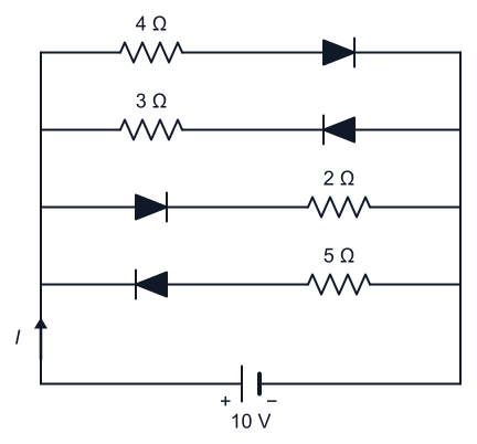
The current in the circuit shown below is: (All diodes are ideal and identical)
- (1)
A
- (2)
A
- (3)
A
- (4)
A
Answer and solution
Answer: (4)
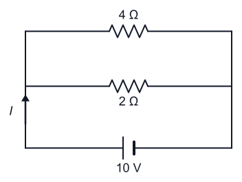
An ideal diode has zero forward resistance and infinite reverse resistance, so only the branches whose diodes are forward biased conduct; here that leaves the 4 and 2 resistors in parallel across the 10 V battery. The current is A, giving (4). The other options wrongly include the reverse-biased 3 and 5 branches that actually carry no current.
- (1)
NEET 2026 · Q18
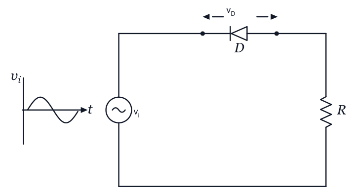
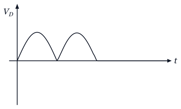
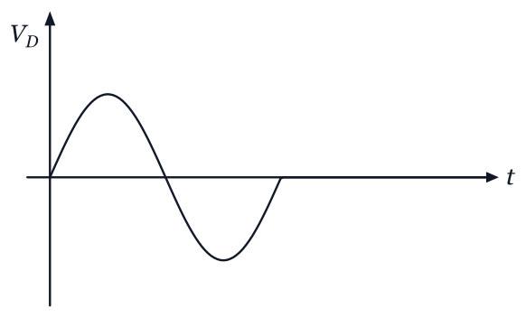
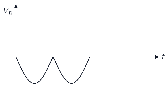
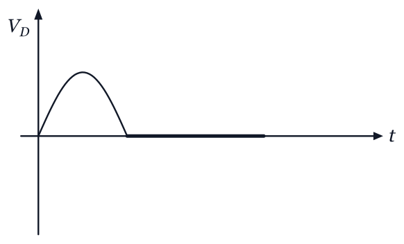
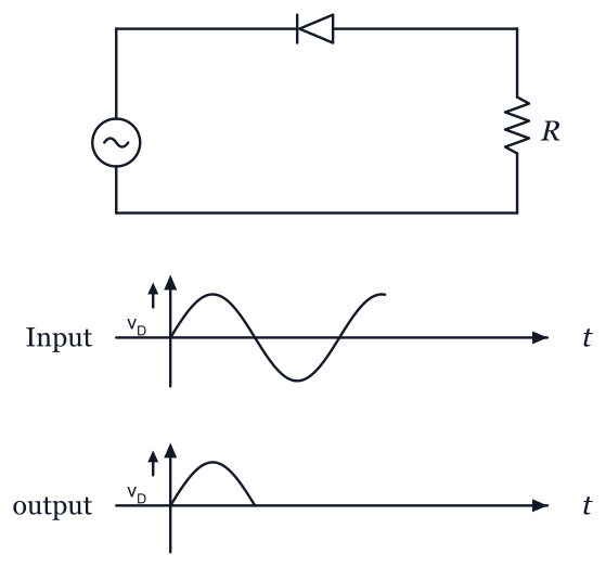
In the circuit shown below, the voltage appearing across the diode will be of the form:
- (1)
- (2)
- (3)
- (4)
Answer and solution
Answer: (4)
The applied alternating current (ac) voltage drives current through the diode and R in series. During the half-cycle that reverse-biases the diode, almost the entire source voltage appears across the non-conducting diode, whereas in the forward-biased half-cycle the diode drop is nearly zero. So consists of one-sided humps with flat (near-zero) gaps, matching option (4). A full sine or a double-hump trace would wrongly imply the diode never blocks the current.
- (1)
NEET 2026 · Q40
Two statements are given below. Choose the correct answer from the options given below.
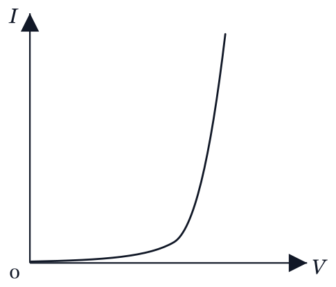
I. A. When the forward bias voltage across a p-n junction diode increases above a certain threshold voltage, the diode current increases significantly.
II. B. This current is called reverse saturation current.- (1)
Both Statements A and B are true
- (2)
Statement A is true, but Statement B is false
- (3)
Both Statements A and B are false
- (4)
Statement A is false, but Statement B is true
Answer and solution
Answer: (2)
Statement A is correct: beyond the threshold (knee) voltage in forward bias, the diode current rises steeply, as seen in the forward V-I characteristic. Statement B is wrong: this rapidly increasing current is the forward current, whereas reverse saturation current is the very small, nearly constant current that flows under reverse bias.
- (1)
Re-NEET 2026
Re-NEET 2026 · Q16
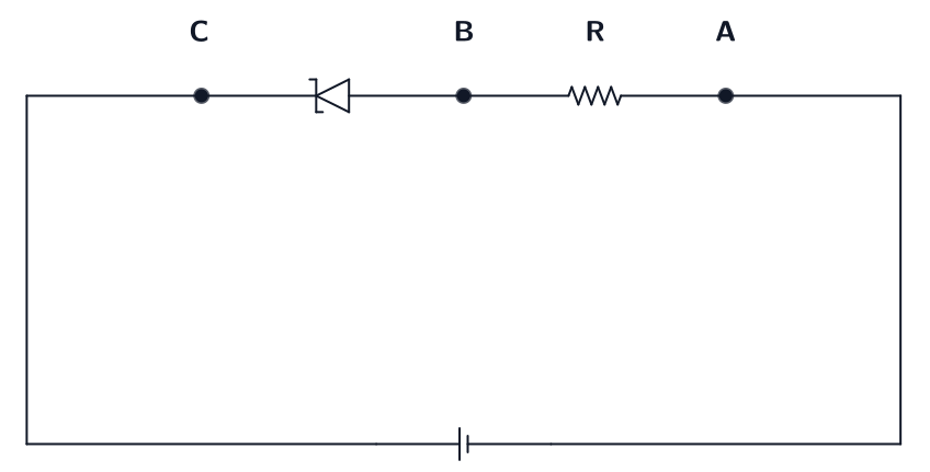
An ideal Zener diode with breakdown voltage of -3 V is reverse biased with a negative input voltage . The magnitude of voltage difference between point and is:
- (1)
3 V
- (2)
2 V
- (3)
1 V
- (4)
0 V
Answer and solution
Answer: (2)
Once an ideal Zener diode is driven past its breakdown voltage it CLAMPS the voltage across itself at 3 V and behaves like a constant-voltage source. The remaining of the supply must therefore appear across the series resistor, which is the element between and . NCERT Class 12, Semiconductor Electronics (Zener diode as a voltage regulator).
Why the other options are wrong:
- (1) reports the voltage across the ZENER rather than across the resistor between and
- (3) subtracts twice, or assumes the diode drops an extra 1 V forward-bias contribution
- (4) assumes the reverse-biased diode blocks all current, so no drop appears across the resistor - but breakdown means current does flow- (1)
Re-NEET 2026 · Q42
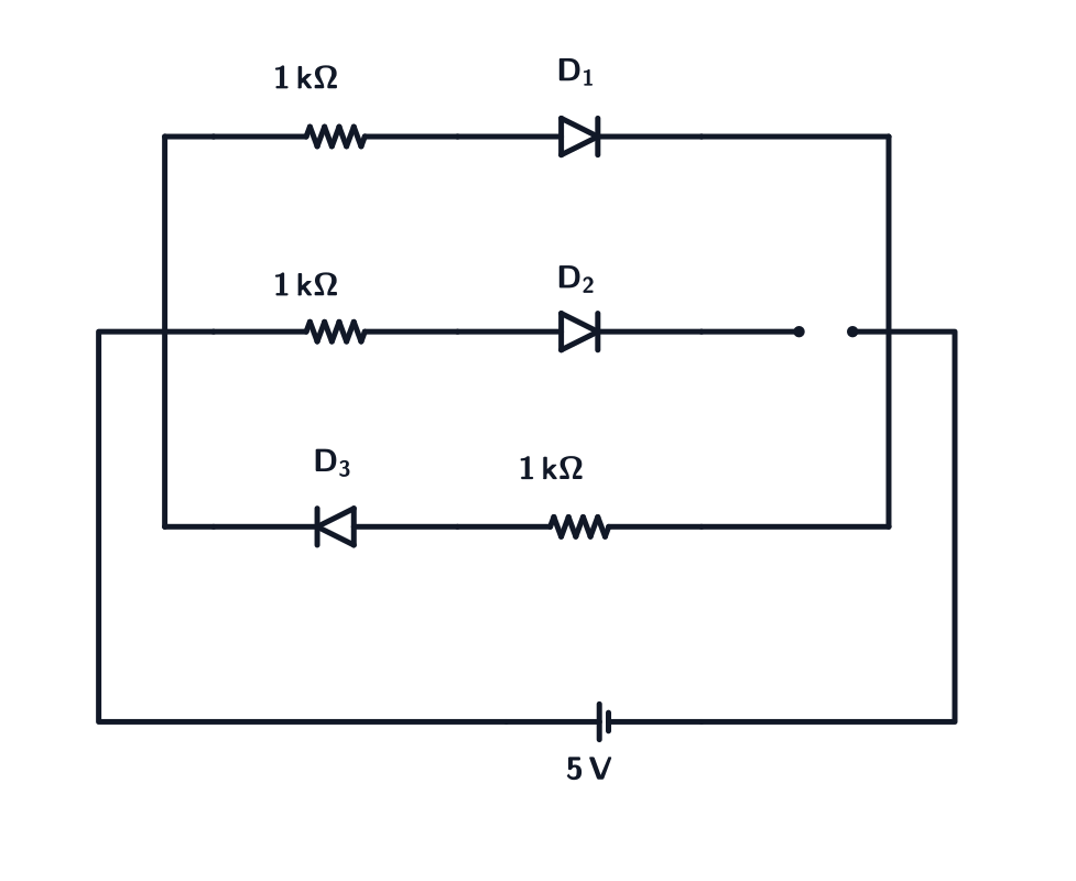
Three identical p-n junction diodes , , and are connected across a battery as shown in the figure. If the width of the depletion regions of , and are , and , respectively, then the correct option is:
- (1)
- (2)
- (3)
- (4)
Answer and solution
Answer: (3)
Depletion width is set by the net potential barrier at the junction. Forward bias lowers the barrier and NARROWS the depletion layer; reverse bias raises it and WIDENS the layer; an unbiased junction sits at its equilibrium width in between. In this circuit is forward biased (narrowest), 's branch carries no bias so it keeps its equilibrium width, and is reverse biased (widest), giving . NCERT Class 12, Semiconductor Electronics (p-n junction).
Why the other options are wrong:
- (1) reverses the bias effect, assuming forward bias widens and reverse bias narrows the depletion region
- (2) assumes forward and reverse bias shift the width by equal and opposite amounts so that and coincide
- (4) treats the unbiased diode as the extreme case rather than the intermediate one- (1)
NEET 2020
NEET 2020 · Q152
The increase in the width of the depletion region in a p-n junction diode is due to :
- (1)
reverse bias only
- (2)
both forward bias and reverse bias
- (3)
increase in forward current
- (4)
forward bias only
Answer and solution
Answer: (1)
The width of the depletion region increases under reverse bias, as the applied voltage enhances the electric field and repels more majority carriers away from the junction. Chapter: Semiconductor Electronics.
- (1)
NEET 2020 · Q167
For transistor action, which of the following statements is correct?
- (1)
Base, emitter and collector regions should have same size.
- (2)
Both emitter junction as well as the collector junction are forward biased.
- (3)
The base region must be very thin and lightly doped.
- (4)
Base, emitter and collector regions should have same doping concentrations.
Answer and solution
Answer: (3)
For transistor action, the base region must be very thin and lightly doped to ensure that most of the charge carriers injected from the emitter reach the collector. Chapter: Semiconductor Electronics.
- (1)
NEET 2020 · Q177
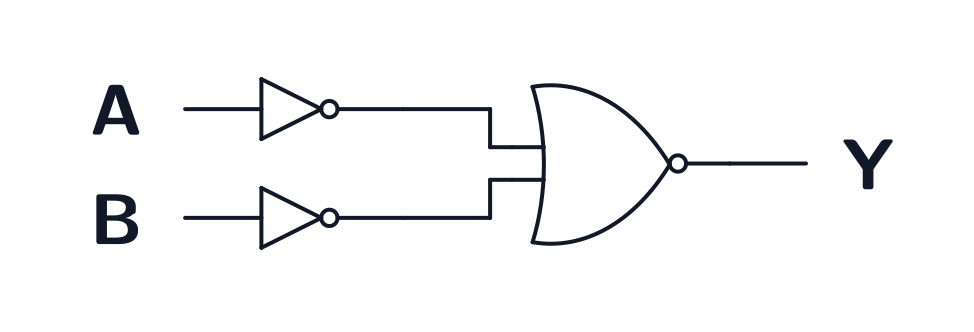
For the logic circuit shown, the truth table is
- (1)
A
B
Y
0
0
0
0
1
1
1
0
1
1
1
1
- (2)
A
B
Y
0
0
1
0
1
1
1
0
1
1
1
0
- (3)
A
B
Y
0
0
1
0
1
0
1
0
0
1
1
0
- (4)
A
B
Y
0
0
0
0
1
0
1
0
0
1
1
1
Answer and solution
Answer: (4)
Each input passes through a NOT gate, and the two inverted inputs feed a NOT-OR (NOR) gate, so Y = NOT(NOT A OR NOT B), which simplifies to A AND B. The circuit is therefore an AND gate, whose output is high only when both inputs are high:
A
B
Y
0
0
0
0
1
0
1
0
0
1
1
1
Chapter: Semiconductor Electronics.
Why the other options are wrong:
- (1) This is the OR truth table: it makes Y high whenever either input is high, which the inverters plus NOR does not do.
- (2) This is the NOT-AND (NAND) truth table, the inverse of the correct one. It would follow from an AND gate with an inverted output.
- (3) This is the NOR truth table, which is what a single NOR gate gives for A and B directly, without the two inverters.- (1)
Practise Semiconductor Electronics in the app: it brings back the questions you get wrong, so the chapter improves, not just your memory of these. Or try the free CBT mock. All chapters: NEET chapter-wise PYQs.
Questions
Are these the official NEET questions on Semiconductor Electronics?
Yes. They are the questions NTA set in each paper, in its wording. The solutions are written by BrainIt.
Something here wrong or out of date? Email hello@brainit.pro and a person will read it.